Nankai University Team Achieves New Breakthrough in Silicon-Based Broadband Photodetection from the Visible to Near-Infrared Spectrum
A research team led by Professors Wu Qiang, Zhou Xu, and Xu Jingjun from the School of Physics, Nankai University, has recently made significant progress in femtosecond-laser hyperdoping technology and silicon-based photodetector, opening a new path for the development of broadband imaging chips.
By integrating pulse-shaping technology with femtosecond-laser hyperdoping, the team has significantly improved the uniformity of surface microstructures and dopant distribution in hyperdoped silicon materials, leading to comprehensive optimization of device detection performance. The detector delivers a breakthrough response in the visible band, and its peak specific detectivity has set a new record among silicon-based photodetectors. The minimum detectable light intensity is more than 200 times lower than that of commercial high-end silicon PIN photodetectors. More importantly, the detector has successfully broken through the traditional 1100 nm detection limit of silicon-based photodetectors and achieved stable response at 1550 nm under room temperature, truly enabling seamless broadband detection from the visible to the near-infrared region. These achievements provide a high-performance, low-cost and easily integrable solution for applications such as autonomous driving, LiDAR, low-light night-vision imaging, and high-precision medical diagnostics.
The related findings were published in International Journal of Extreme Manufacturing, a prestigious international academic journal in engineering and manufacturing, under the title “Pulse-shaped femtosecond-laser-modified Si:S photodetector for ultrawide-spectrum focal plane arrays and weak-light detection”. Nankai University is the first-author institution, and the first author is Cao Jiaxin, a doctoral student at Nankai University.
The team has long been committed to advancing the application of femtosecond-laser hyperdoping technology in the semiconductor and optoelectronics. In recent studies, the team has also proposed femtosecond-laser planar hyperdoping technology and a combined approach that integrates femtosecond-laser doping with nanosecond-laser activation. These advances have successfully resolved the key compatibility issue between femtosecond-laser doping and advanced-node chip manufacturing processes, making it promising to extend to a broader range of semiconductor materials and chip platforms and become a standard fabrication process in next-generation chip manufacturing.
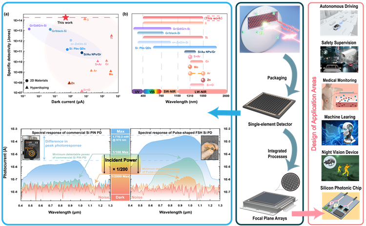
Fig. 1 Design of application areas for pulse-shaped fs-laser-modified Si:S photodetectors and schematic diagram of the processing system
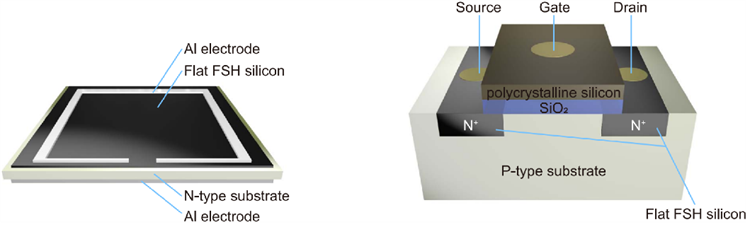
Fig. 2 Application design of planar femtosecond-laser-modified silicon in CMOS processes
Link to the paper:
https://iopscience.iop.org/article/10.1088/2631-7990/ae3b83/meta
(Edited and translated by Nankai News Team.)
38 Tongyan Road, Jinnan District, Tianjin, P.R.China 300350 94 Weijin Road, Nankai District, Tianjin, P.R.China 300071
Copyright: Nankai University All Rights Reserved